



晶圆研磨切割设备 Wafer Grinding Dicing
HURAKAN全程主导晶圆研磨切割设备全流程工业设计与量产落地工作,深度对标半导体晶圆加工行业严苛标准,贴合芯片制造、晶圆封装、精密切割研磨等无尘车间工况要求,联动客户研发、精密工艺、量产生产团队开展全维度需求攻坚与方案打磨。针对设备高精度切割研磨、晶圆防护防损、整机无尘密闭、精密模组防震、腔体清洁维保、半导体产线适配等核心落地难点,逐一校核整机钣金公差、内部精密模组堆叠、腔体密封结构、防震固定工艺与拆装适配标准,经过多轮精密工况仿真、无尘环境实测、样机迭代调校与量产工艺优化,有效解决传统晶圆加工设备结构松散、防尘密闭性差、维保拆装繁琐、精密工况适配性不足等行业量产痛点,以严谨扎实的全链路落地实操能力,保障所有设计方案完全贴合半导体量产规范,实现设计图纸与终端量产设备的精准还原落地。
HURAKAN took the lead in the full-process industrial design and mass production implementation of wafer grinding and cutting equipment. We strictly complied with the stringent standards of the semiconductor wafer processing industry, adapted to the clean workshop working conditions of chip manufacturing, wafer packaging and precision cutting and grinding, and carried out full-dimensional demand research and scheme optimization with the client’s R&D, precision process and mass production teams. Focusing on core difficulties such as high-precision cutting and grinding, wafer damage prevention, overall dust-free sealing, precision module shockproof, cavity cleaning and maintenance, and semiconductor production line adaptation, we verified overall sheet metal tolerance, internal precision module stacking, cavity sealing structure, shockproof fixing process and disassembly adaptation standards one by one. Through multiple rounds of precise working condition simulation, dust-free environment testing, prototype iteration and process optimization, we solved common mass production pain points of traditional wafer processing equipment, ensuring all design schemes fully conform to semiconductor mass production specifications and realize accurate implementation from design drawings to terminal equipment with solid full-link practical capabilities.
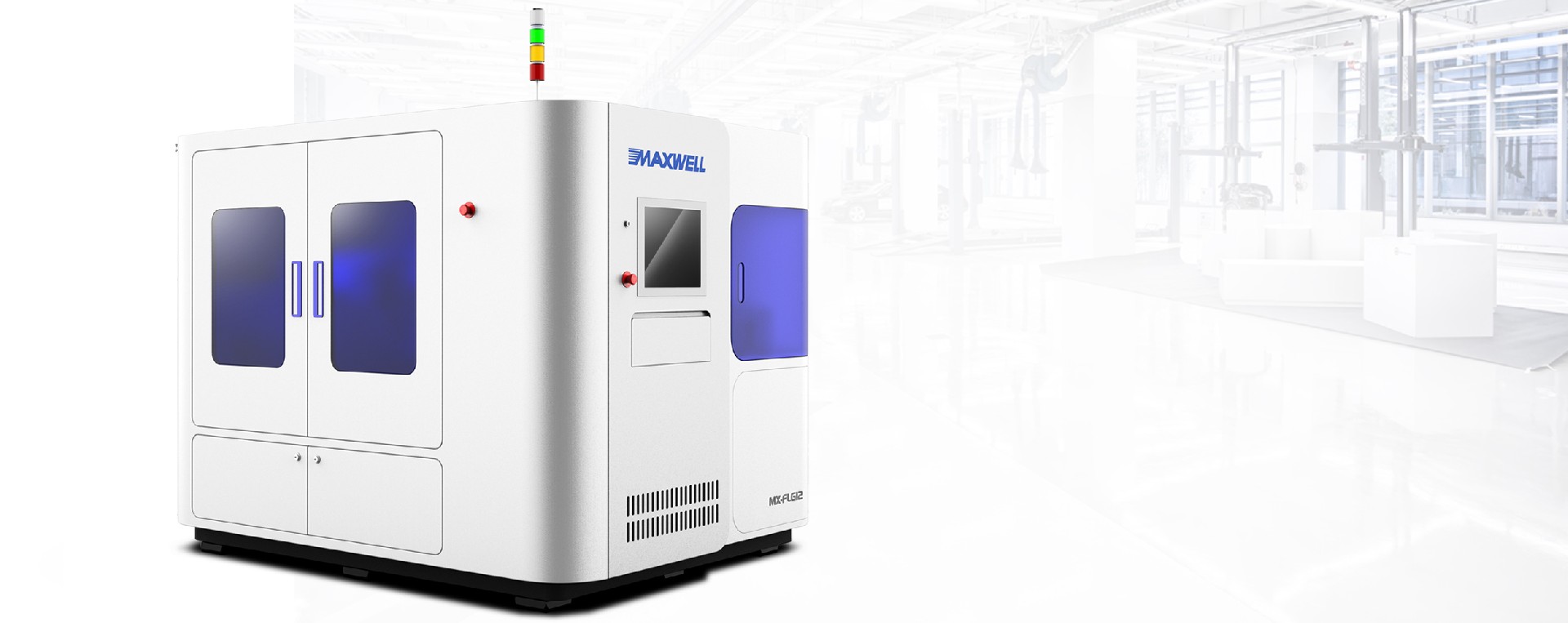
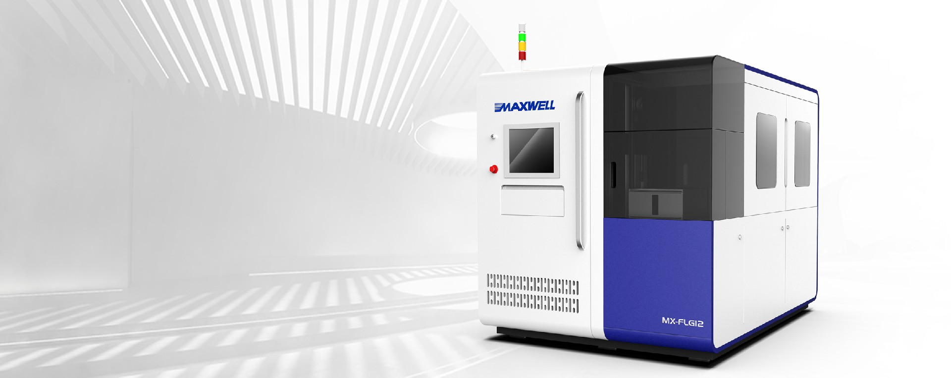
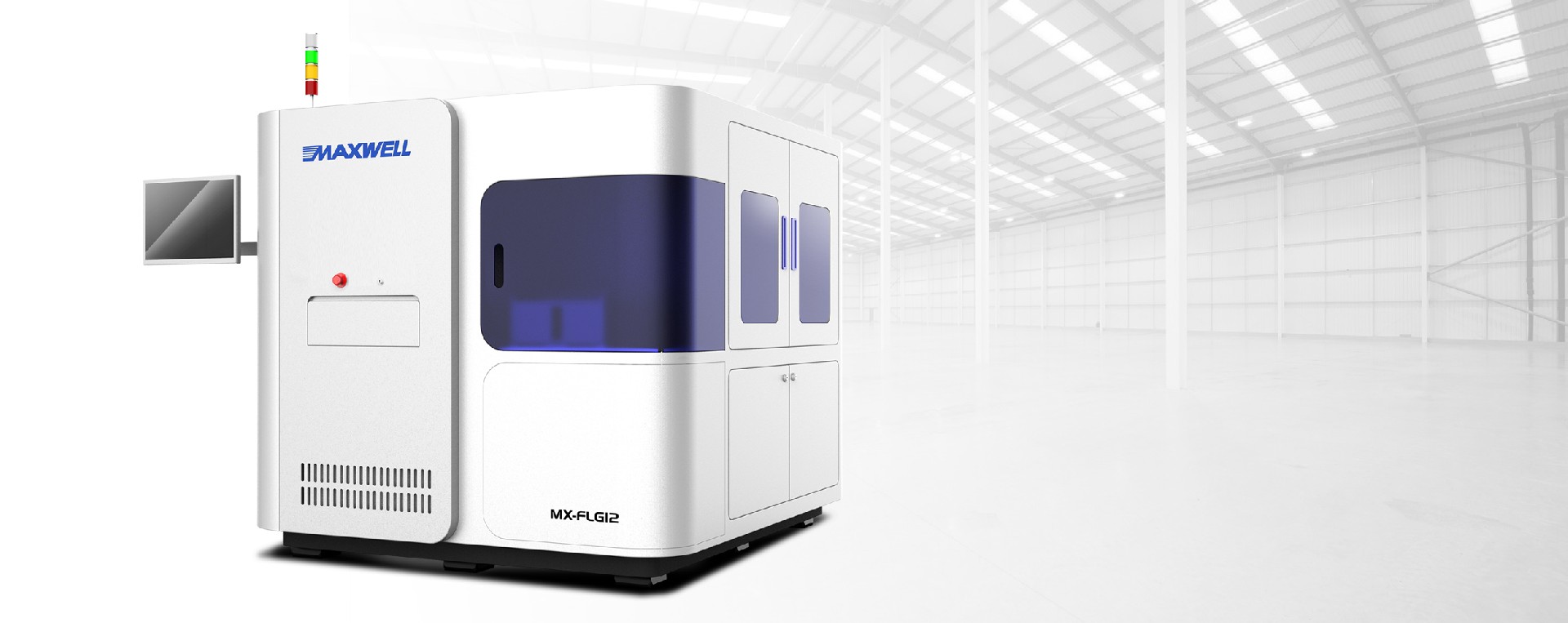
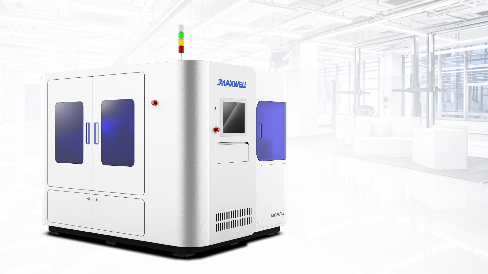
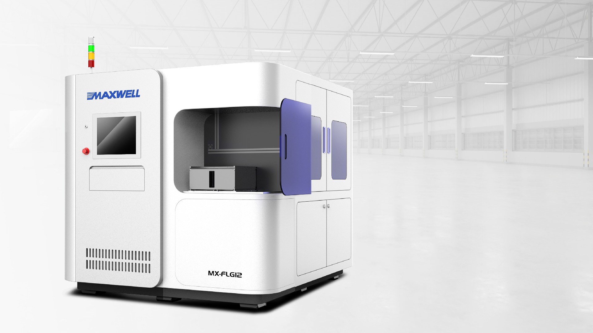
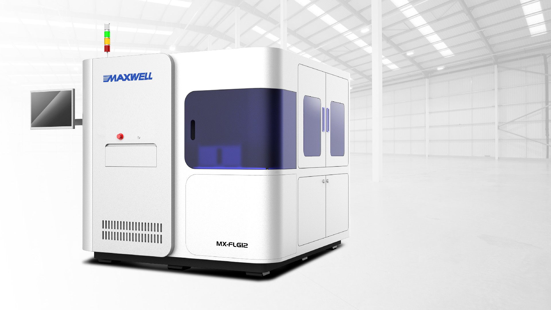
HURAKAN打破传统晶圆研磨切割设备造型厚重刻板、结构布局杂乱、密闭防护不足、人机操作繁琐的行业短板,完成造型、结构与人机交互全方位创新升级。造型层面摒弃传统半导体设备笨重生硬的工业化外观,采用一体化极简规整机身设计,优化整机比例与立面层次分割,线条简约硬朗且极具秩序感,弱化重型精密设备的厚重感,兼具半导体设备的专业严谨性与高端智能装备的科技质感,完美适配半导体无尘车间、精密芯片加工工位等高端场景调性;结构层面采用模块化分区集成架构,将研磨模组、切割动力单元、精密传动系统、电控散热腔体有序分区整合,优化内部风道、除尘结构与防震布局,最大程度规避粉尘、震动对晶圆加工精度的干扰,同时优化腔体开合与模组拆装结构,大幅提升设备内部清洁、耗材更换、精密部件校准维保效率,强化整机密闭防尘、抗震稳控性能,适配半导体行业长期高精密连续作业需求;人机交互层面贴合半导体工程师调试、参数标定、工况监测、故障排查的作业习惯,优化触控面板安装高度、屏幕倾角与功能分区,精简精密参数调节、设备启停、工况数据可视化、故障溯源等操作逻辑,降低专业操作门槛,减少高精度作业失误率,有效缓解长期值守疲劳,全方位提升精密加工作业效率与安全性。
HURAKAN breaks the industry shortcomings of traditional wafer grinding and cutting equipment such as heavy and rigid shape, disordered structural layout, insufficient closed protection and cumbersome human-computer operation, realizing all-round innovative upgrades in shape, structure and human-computer interaction. In terms of shape, it abandons the bulky and rigid industrial appearance of traditional semiconductor equipment, adopts an integrated minimalist and regular body design, and optimizes overall proportion and facade division. The simple and tough lines present a strong sense of order, reducing the heaviness of heavy precision equipment and balancing the professional rigor of semiconductor equipment and the technological texture of high-end intelligent equipment, which perfectly adapts to high-end scenarios such as semiconductor dust-free workshops and precision chip processing stations. In terms of structure, the modular zoning integrated architecture orderly integrates grinding modules, cutting power units, precision transmission systems and electronic control heat dissipation cavities, optimizing internal air ducts, dust removal structures and shockproof layouts to minimize the interference of dust and vibration on wafer processing accuracy. The optimized cavity opening and module disassembly structure greatly improves the efficiency of internal equipment cleaning, consumable replacement and precision component calibration and maintenance, and strengthens the overall closed dust-proof and shock-resistant performance to adapt to long-term high-precision continuous operation in the semiconductor industry. In terms of human-computer interaction, we optimize the touch panel height, screen inclination and functional zoning according to the operation habits of semiconductor engineers, simplify the operation logic of precision parameter adjustment, equipment start-stop, working condition data visualization and fault tracing, reduce professional operation thresholds and error rates in high-precision operation, alleviate long-term on-duty fatigue, and comprehensively improve the efficiency and safety of precision processing operations.
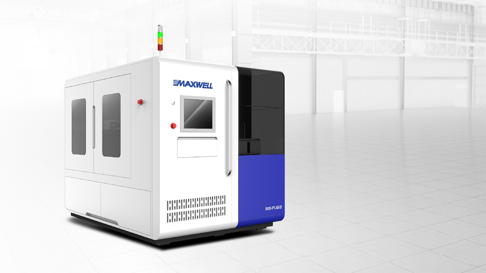
本次专业化差异化设计彻底打破了半导体精密加工设备行业同质化严重、外观粗放、体验滞后、依赖硬件参数低价内卷的市场格局,以规整高端的整机造型、稳定精密的模块化结构、安全高效的人机运维体验,构筑产品专属核心差异化竞争壁垒。让设备彻底摆脱传统工业精密设备的同质化工具标签,树立精细、智能、高端的半导体专业设备形象,帮助客户跳出行业低价竞争泥潭,形成颜值、精度、体验三位一体的核心市场卖点,为产品实现稳定高端溢价、夯实品牌在半导体精密设备领域的专业话语权提供核心设计支撑。
This professional differentiated design completely breaks the market pattern of serious homogenization, extensive appearance, backward experience and low-price involution relying on hardware parameters in the semiconductor precision processing equipment industry. It builds exclusive core differentiated competitive barriers with neat and high-end overall shape, stable and precise modular structure, and safe and efficient human-machine operation and maintenance experience. The product completely gets rid of the homogenized tooling label of traditional industrial precision equipment, establishes a sophisticated, intelligent and high-end professional image of semiconductor equipment, helps clients get out of the industry low-price competition quagmire, form three-dimensional core market selling points of appearance, precision and experience, and provide core design support for stable high-end premium and consolidated professional discourse power in the field of semiconductor precision equipment.
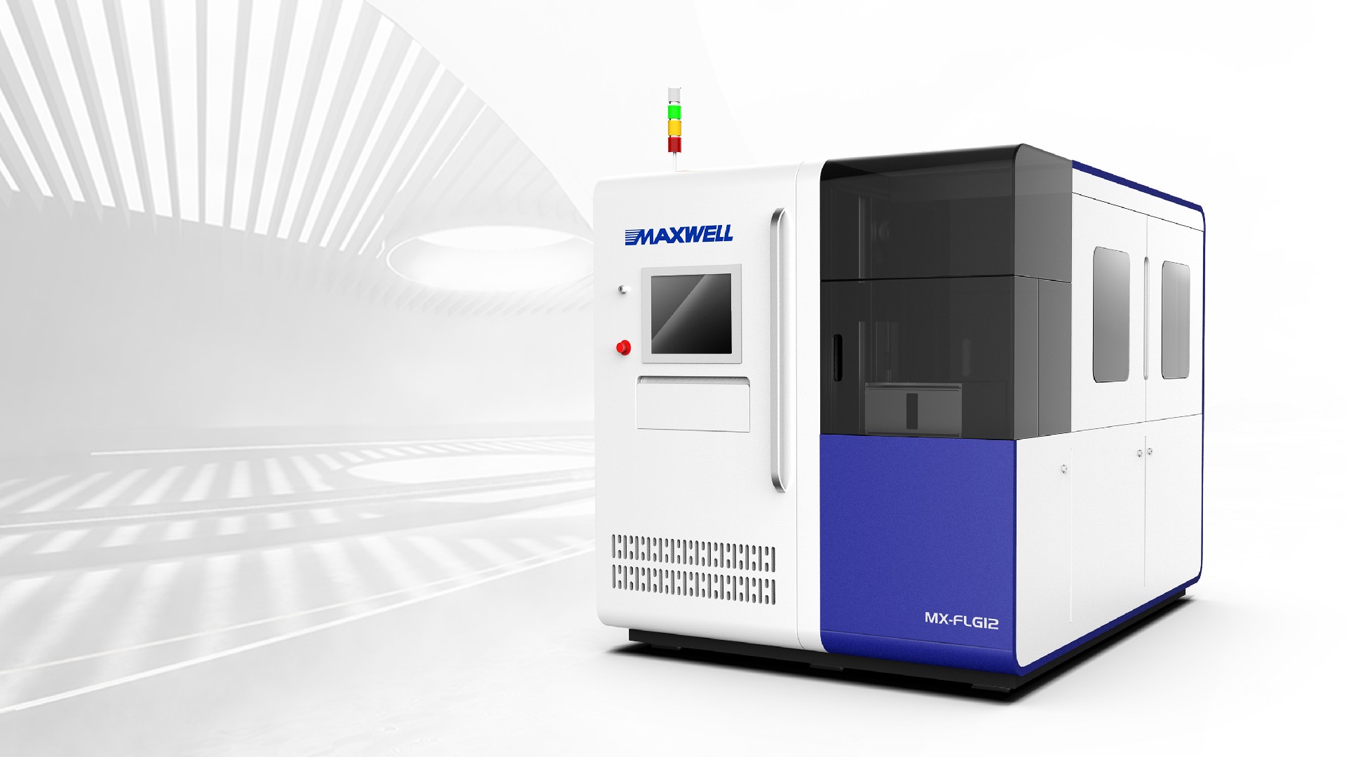
设备量产投放市场后,凭借精致专业的整机外观、超高精度的加工性能、稳定的无尘密闭防护能力与低运维成本,快速获得晶圆制造、芯片封装、半导体精密加工等头部企业的高度认可,批量采购与项目定制订单持续攀升。相较于客户上一代机型,新品市场询价率、中标率与客户复购率大幅提升,成功切入中高端半导体精密设备采购供应链,拓宽国家级科创实验室、头部芯片厂商、半导体产业园配套等优质高端销售渠道,持续提升细分赛道市场占有率与行业核心竞争力。
After mass production and launch, the equipment has been highly recognized by leading enterprises in wafer manufacturing, chip packaging and semiconductor precision processing with its exquisite and professional appearance, ultra-high-precision processing performance, stable dust-free closed protection capability and low maintenance cost, with bulk procurement and project customized orders growing steadily. Compared with the client’s previous generation models, the new product has a significant increase in market inquiry rate, bidding success rate and customer repurchase rate. It has successfully entered the mid-to-high-end semiconductor precision equipment procurement supply chain, expanded high-end sales channels such as national science and innovation laboratories, leading chip manufacturers and semiconductor industrial park supporting projects, and continuously improved market share and core industry competitiveness in the segmented track.
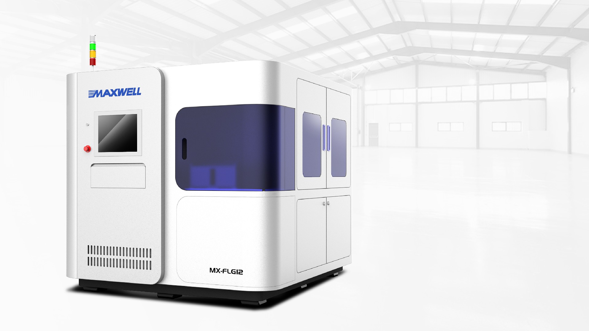
HURAKAN始终以量产落地为核心、市场价值为导向,深耕半导体精密智能设备设计领域,平衡工艺落地性、精密结构可靠性、设计创新性与半导体场景专属实用性,为高端晶圆研磨切割设备打造可量产、高精密、高溢价的全链路工业设计解决方案,持续助力合作客户夯实产品技术与形象双重竞争壁垒,升级品牌行业高端定位,实现长效稳定的商业营收增长与行业市场地位跃升。
Centering on mass production implementation and oriented by market value, HURAKAN deeply cultivates the field of semiconductor precision intelligent equipment design, balancing process implementability, precision structural reliability, design innovation and exclusive practicality for semiconductor scenarios. We create mass-producible, high-precision and high-premium full-link industrial design solutions for high-end wafer grinding and cutting equipment, continuously helping cooperative clients consolidate dual competitive barriers of product technology and image, upgrade the high-end industry positioning of the brand, and achieve long-term and stable commercial revenue growth and leapfrog improvement of industry market status.



Microblog